MIPS CPU with a single clock cycle
The MIPS architecture is of type RISC and originated in 1981 from a research project by Prof. Hennessy at Stanford. This architecture is characterized by instructions of the same length, and is geared toward simplifying pipeline implementation.
In this post we will see and comment the schematic of the single clock cycle MIPS CPU, to understand what certain functional units are used for.
Here is the simplified schematic of a one-shot-clock MIPS CPU.
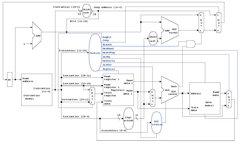
It may seem complex at a first glance, but after some exploration, it gets better.
Clock cycle phases
As a start, it is useful to keep in mind the steps in the execution of an instruction:
- Fetch: the instruction is taken from instruction memory;
- Decode: the instruction is unpacked, and the individual pieces take on their meaning;
- Execute: the ALU performs a calculation;
- Memory: eventually the ALU’s result or read from a register is written to memory, or memory is read;
- Write-Back: possibly the result of the ALU or the read from memory is written to a register.
Now it’s pretty quick to see similarities with the pattern:
- Fetch: includes the PC (Program Counter) and the nearby adder;
- Decode: includes unpacking the instruction, the control unit, and reading from registers;
- Execute: covers the part where the ALU operates;
- Memory: access to data memory;
- Write-Back: the output of the lower-right mux.
Instruction format
In the MIPS architecture we have 3 types of instructions: R, I, J. I elaborate on this in the MIPS assembly post, but for the purpose of this explanation we only need the instruction format in general.
Some arguments are common between R and I, while others vary depending on the format. Let’s clarify:
oc: is the opcode of the instruction, that is, a code that identifies it (and thus determines its format);rs: source register;rt: target register;rd: destination register;shamt: shift amount*; if the operation is a shift, it represents the number of positions to be shifted;func: together with the control signalAluOpdetermines the function to be passed to the ALU;imm: immediate part, i.e., a constant;dest: constant indicating the address to jump to.
Control signals
After reading the opcode, the control unit activates appropriate control signals so that the CPU behaves well. On the schematic, the control signals are highlighted in blue, and are:
RegDst: chooses the target register betweenrdandrt. It is useful because it allows the two encodingsRandIto be supported without adding too much circuitry. Simply, depending on the format one of the two arguments is chosen as the destination;Jump: active if the instruction is from thejumpfamily;Branch: active if the instruction is from thebranchfamily;MemRead: active if the instruction reads from memory;MemToReg: active if the data read from memory is to be slapped into a register;AluOp: identifies the operation to be performed by the ALU (I carry over instructions):00:addi,lw,sw;01:beq,bne;1x: depends on thefuncfield:32:add;34:sub;36:and;37:or;42:slt.
MemWrite: active if the instruction writes to memory;AluSrc: active if the second operand of the ALU is to be theimmfield;RegWrite: active if the instruction writes to a register.
Very nice. Now all the control signals make sense and don’t scare us anymore; so we can move on.
Schema Analysis
Let’s break the pattern into blocks, and comment on it.
Fetch
In this step we need to fetch the next instruction from instruction memory. We know that all instructions are one word (4 bytes) long, so we have a nice adder that just does the current_address + 4 calculation;
The handling of jumps or branches happens in the next step, that is, when we have the control signals well set up.
Decode
Here we have to pack the instruction and based on the oc activate the appropriate control signals. Let’s take a closer look at how the CPU behaves.
Branch and Jump
Here it is convenient to analyze these two control signals together to see how the PC alters:
- If
Branchis active, it means we have to jump if the condition is true. The condition check is done by the ALU with a difference between the values of the two registers to be checked. If the result is0it means that the condition is verified, and therefore we have to skip. For this we haveBranch AND 0which activates the mux that chooses between the result of the adder seen before, and the relative address of the jump; - If
Jumpis active, we have to jump to the address contained in thedestfield, so thePCis updated with the jump address.
Quick question: *what happens if Jump and Branch are both active?
Now based on the values of the instruction fields, data is read from the registers.
Execute
We have the arguments of the ALU and the operation to execute. The ALU calculates, and the result can represent:
- The address to read from in RAM;
- The jump enable of a branch;
- A value to be written to a register.
Memory
Based on what was said just now and the control signals, it can either read or write.
Write-Back
Simply:
- If
MemToRegis active, the read data is thrown directly into the destination register; - Otherwise, the result of the ALU is written.
Recap
To conclude, today we found out:
- What a MIPS CPU with a single clock cycle looks like.
- What the execution stages are.
- What control signals exist, and how they are activated.
- How control signals affect the execution flow.
- That control signals are important.